I'm getting close to making the LCDs work from Ben's Micro 2700 POS terminals (several of them are still up for grabs). Here's a photo.
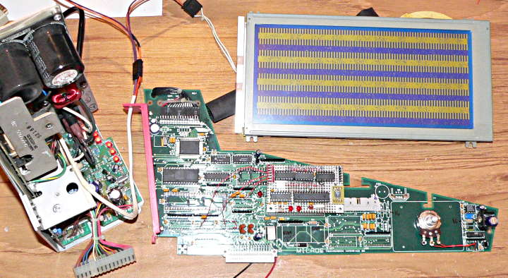
More photos and technical details below...
First, I cut out almost all the chips. Here's a photos taken before I chopped all the chips off.
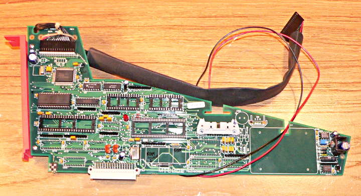
Really only 3 chips in the upper left corner are needed, the MSM6255 controller chip, the 32k RAM chip, and a 74HCT245 tri-state buffer. (those other 2 chips I left in place are buffers and transistors which seem to do startup stuff like reset pules and switching the RAM chip from battery backup to main power).
The MSM6255 has two buses, both 8 bit data, 16 bit addresses. One bus is for the Z80 microcontroller, and the other is a dedicated bus for the frame buffer RAM chip. The LCD controller only has 9 configuration registers, and a single instruction register. It only listens on 1 of the 16 address lines, which select between the instruction register or the 9 config registers. To write to the chip, you write to instruction register with A0=1, with the number of the config register you want. Then you write again with A0=0 to configure. Repeat this process 9 times to configure everything. However, a few of the registers only matter in character mode, and this board is wired only for graphical mode.
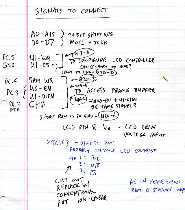
Since there are no other chips on the Z80 bus, I just wired the LCD controller chip select low (fount at U20, pin 10), and then it only takes 1 write select signal (found at U13, pin 11) to strobe the data in. Of course, A0 and the 8 data lines have to correct before pulsing the write pin low.
To access the frame buffer, the is a 74HCT245 tri-state buffer which causes the Z80 data lines to drive the frame buffer data lines. The LCD controller also has an address mux controlled by the DIEN signal. Both of these fortunately are high for the controller to access the frame buffer and low when the Z80 bus drives the RAM. So I just shorted them together (found at U19, pin 2 and 11). The RAM has its read signal low all the time. All I had to do was short the RAM CS signal low (found at U20, pin 6) to allow it to work.
The RAM write signal takes priority over read, so when you want to write new data into the frame buffer, all that's necessary is to drive DIEN and the '245 enable low to connect the Z80 bus to the frame buffer RAM (of course, set up the desired address and data first), and then pulse the RAM write signal low.
The frame buffer can be written at any time this way, but if this also happens to be at a moment when the LCD controller is reading, the screen will momentarily display whatever was on the frame buffer RAM data lines being driven by the 74HCT245 buffer. It appears this is the way the Micros 2700 worked.
The datasheet gives two suggestions for detecting times when the LCD controller isn't reading the data lines, and one of them isn't practical for large displays like this one. The other basically involves watching the CH0 signal from the controller and doing the framebuffer access right after it changes. I could not find the CH0 signal routed anywhere on the board, so I'm pretty sure Micros just didn't use it (they certainly didn't build the complex flip-flop sync circuit suggested in the MSM6255 datasheet). Maybe when I've got everything figured out I'll wire CH0 to a port pin and write a bit of code that waits for it to change right before I do the framebuffer write. It looks like CH0 is about a 560 kHz square wave, so that's plenty of time for a tight loop in the 18.432 MHz AVR to detect and complete the access. But for now, I'm not worrying about CH0.
So, here's my little circuit.
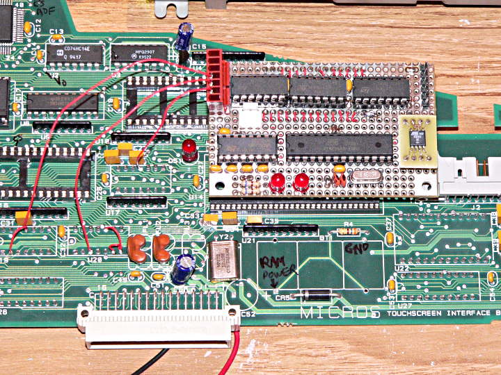
On the top are three 74HC164 shift register chips. These are connected to the MOSI and SCLK signals, so whatever the last 3 bytes were on the SPI port, they end up driving the Z80 address and data bus. The board has two headers that plug into the socket for the RAM chip that was dedicated to the Z80, so power, ground and all the address and data lines are connected there. That just leave the 2 write strobes for the LCD controller and frame buffer RAM, and the enable signal to drive the frame buffer bus. Only 3 extra signals! Well, maybe a 4th when/if I connect CH0 to avoid flicker.
The 28 pin chip is a ATMEGA88 - the same chip as the Aurdino, but only 8k of program memory. The chip on the left is a MAX232, and the white 3 pin connector is for a serial port that is intended to (someday) allow images to be downloaded easily. The little 8 pin chip on the right right is a 128K flash rom with SPI interface (Atmel AT45D011), which can hold 8 full-screem images, when I get all the pixels under control!
But not everything is working perfectly... yet. Here's what I get so far, trying to fill the entire frame buffer with 0x0F.
Those vertical bars are the desired pixels. They do change to other patters if I fill the frame buffer with other bytes. So at least I'm controlling some pixels.
Clearly, I haven't got the correct configuration for the LCD controller yet. The controller is designed to drive 2 sets of shift registers on the LCD, with 1, 2 or 4 bits per. This LCD seems to have only 1 shifter register with 4 bits, so I'm not entirely sure if I should use 2 or 4 bit mode, and exactly what the duty cycle setting should be isn't clear either. I've tried many different settings (mostly randomly), and so far none have been perfect.
I'll probably do one more session with the ohm meter to figure out more about how the LCD interfaces to the controller, and details about the frame buffer bus (which so far I've assumed is wired like the datasheet describes, but really all my probing has been on the Z80 bus and the many control signals).
Here are my latest notes/scribbles about how to connect the various signals.
I should also mention the stuff I learned about the power supply.
First, the simple part, the backlight. It's a cold cathode florescent lamp, and there is a module inside the main power supply. It's attached to the high voltage board deep inside, and so far I've just left it alone. I did stick my meter probe in there (past all the live 120 volt stuff in the way), and it looks like that module takes 24 volts DC input. Not at nice as 5 volts, but still not too bad. It looks like it can be easily separated and liberated from the big hulking power supply. The one sad bit is there is only 1 in there, with a Y cable to drive both LCDs.... so if everyone wants one of these LCDs for a project, half of them will need to acquire or build a CCFL driver.
The not-as-simple part (but still a lot simpler than the LCD config and frame buffer bus) is the LCD drive voltage. The LCD runs on 5 volts for its logic, and a negative voltage, up to -19 volts. The parts on the far right side of the board are a little switching power supply that converts +5 into a variable negative voltage.
At first I thought the little blue trim pot was the answer, but I kept getting very random results, especially if I touched the board. It turns out the chip in the lower right corner is a X9C103 digitally controlled pot, which adjusts the LCD drive voltage (which is what controls the contrast). I thought about hooking it up to the microcontroller, but in the interest of getting this thing to work, I simply clipped it off the board and wiring in a connection 10K pot, which you can see in the photo. However, the digital control pot is there on the board, so when/if anyone else uses all this, it's possible to control it from software. The X9C103 contains EEPROM memory to store the pot setting. I must have changed mine hundreds of times while touching the floating inputs with my fingers and wondering what I was doing that changed the LCD so much!
I had hoped to get this thing working before the next Dorkbot meeting, but it looks like I might have to put this whole thing on the shelf for a couple weeks (to make room for a paying project - which funds all this fun stuff....) I'm pretty sure I'll get the LCD config and frame buffer issues worked out, and when I do it's my hope everyone in Portland Dorkbot who wants one of these displays can have one!